- 您现在的位置:买卖IC网 > Sheet目录1992 > CYW173SXC (Silicon Laboratories Inc)IC CLK GEN TAPE DRV 4CH 16SOIC
W173
......... Document #: 38-07313 Rev. *B Page Page 2 of 5 of 5
Note:
1. All inputs, except X1 or X2, have an internal pull-up resistor. Unconnected inputs will assume a logic HIGH condition.
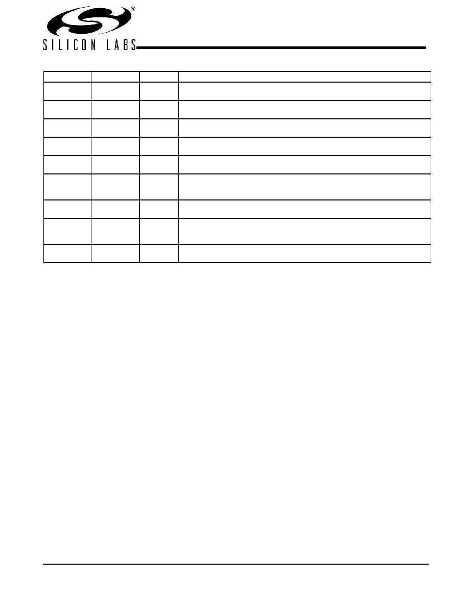
Pin Definitions [1]
Pin Name
Pin No.
Pin Type
Pin Description
OE
5
I
Output Enable: When LOW, this input signal puts all outputs into a high-impedance
state.
13.2MHZ
13
O
Clock Output: Provides a TTL-level timing signal proportional in frequency to the
input signal. For a 26.5625 MHz reference, the frequency will be 13.2 MHz.
6.6MHZ
15
O
Clock Output: Provides a TTL-level timing signal proportional in frequency to the
input signal. For a 26.5625 MHz reference, the frequency will be 6.6 MHz.
10MHZ
10
O
Clock Output: Provides a TTL-level timing signal proportional in frequency to the
input signal. For a 26.5625 MHz reference, the frequency will be 10.0 MHz.
50MHZ
7
O
Clock Output: Provides a TTL-level timing signal proportional in frequency to the
input signal. For a 26.5625 MHz reference, the frequency will be 50.0 MHz.
X1
2
I
External Crystal Connection: This pin has dual functions. It can be used as an
external 26.5625 MHz crystal connection or as an external reference frequency
input.
X2
3
O
External Crystal Connection: An input connection for an external 26.5625 MHz
crystal. If using an external reference, this pin must be left unconnected.
VDD
1, 6, 9, 12, 16
P
Power Supply Connections: Connect both VDD pins to the same voltage, either
3.3V or 5.0V. Each VDD pin should have a decoupling capacitor (such as 0.1 F)
placed as close to the pin as possible.
GND
4, 8, 11, 14
G
Ground Connections: Connect all ground pins to the common system ground
plane.
发布紧急采购,3分钟左右您将得到回复。
相关PDF资料
CYW305OXC
IC CLOCK W305 SOLANO 56SSOP
DAC5674IPHPG4
IC DAC 14BIT 400MSPS 48-HTQFP
DAC7621EBG4
IC SNGL 12BIT PARALLEL D/A 20SSO
DAC7801KPG4
IC DUAL 12BIT CMOS DAC 24-DIP
DAC8043AESZ
IC DAC 12BIT MULT SRL INP 8SOIC
DAC8043GP
IC DAC 12BIT MULTIPLY CMOS 8-DIP
DAC8221GP
IC DAC 12BIT DUAL W/BUFF 24-DIP
DAC8222GPZ
IC DAC 12BIT DUAL W/BUFF 24DIP
相关代理商/技术参数
CYW173SXCT
功能描述:时钟发生器及支持产品 Tape Media Backup Dr Clk Gen W173 DS RoHS:否 制造商:Silicon Labs 类型:Clock Generators 最大输入频率:14.318 MHz 最大输出频率:166 MHz 输出端数量:16 占空比 - 最大:55 % 工作电源电压:3.3 V 工作电源电流:1 mA 最大工作温度:+ 85 C 安装风格:SMD/SMT 封装 / 箱体:QFN-56
CYW180-01SX
制造商:CYPRESS 制造商全称:Cypress Semiconductor 功能描述:Peak Reducing EMI Solution
CYW180-01SXT
制造商:CYPRESS 制造商全称:Cypress Semiconductor 功能描述:Peak Reducing EMI Solution
CYW180-02SX
制造商:CYPRESS 制造商全称:Cypress Semiconductor 功能描述:Peak Reducing EMI Solution
CYW180-02SXT
制造商:CYPRESS 制造商全称:Cypress Semiconductor 功能描述:Peak Reducing EMI Solution
CYW180-03SX
制造商:CYPRESS 制造商全称:Cypress Semiconductor 功能描述:Peak Reducing EMI Solution
CYW180-03SXT
制造商:CYPRESS 制造商全称:Cypress Semiconductor 功能描述:Peak Reducing EMI Solution
CYW180-51SX
制造商:CYPRESS 制造商全称:Cypress Semiconductor 功能描述:Peak Reducing EMI Solution